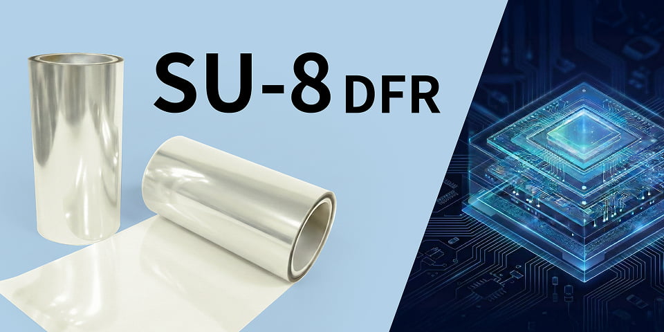
SU-8 DFR Series
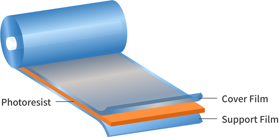
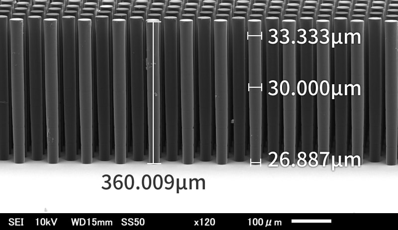
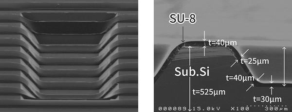
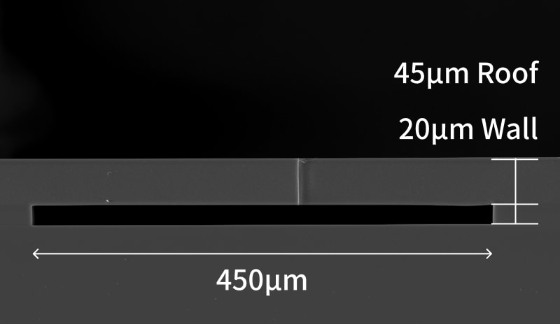
The SU-8 DFR Series is an epoxy-based dry film resist designed for forming high-aspect-ratio structures.
Information may be obtained or stored in your browser by cookies when you access the Website. This information is related to the user, the user settings or device. It is primarily used to ensure the site functions as expected by the user. We respect your right to privacy. Therefore, you can select to not allow some types of cookie. Please click on the different category headings to check the details and then change our default settings.
Strictly Necessary Cookies are cookies that are essential for this site to function properly. Strictly Necessary Cookies do not store information that can identify individuals. Strictly Necessary Cookies are used to view this site. Therefore, you cannot refuse the use of Strictly Necessary Cookies from these cookie settings. However, you can refuse the use of Strictly Necessary Cookies from the settings of your browser at any time. Please note that parts of the site may not function if you refuse the use of Strictly Necessary Cookies.
This site uses the following Strictly Necessary Cookies.
Cookie name: gdprCookieEn
Cookie name: optGA
Cookie name: optPardot
A photoresist is a photosensitive material used in semiconductor and printed circuit board manufacturing. When exposed to light—typically ultraviolet—it undergoes a chemical reaction that changes its properties. This reaction allows the material to function as a mask for transferring fine patterns onto a substrate.
Photoresists are classified into two types:
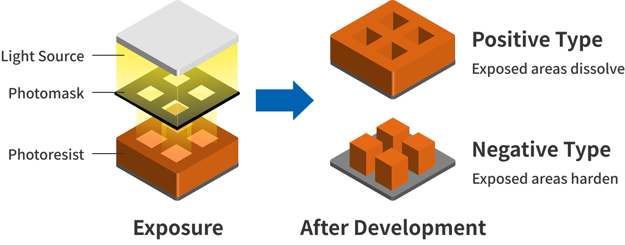
Dry Film Resists (DFR)
(Film type resists laminated onto the wafer)
Liquid Photoresists
(Liquid photoresists coated onto the wafer by spin coating)
Dry film resists are photosensitive materials that enable easy fabrication of cavity structures and other 3D patterns. They are well-suited for applications such as SAW/BAW RF filters that require precise, three-dimensional patterning. After lamination, the film behaves similarly to liquid photoresists and can be removed with standard solvents. This enables high-aspect-ratio, high-resolution patterning. Dry films also eliminate the need for edge-bead removal and provide uniform thickness, helping streamline the manufacturing process.
The SU-8 DFR Series is an epoxy-based dry film resist designed for forming high-aspect-ratio structures.
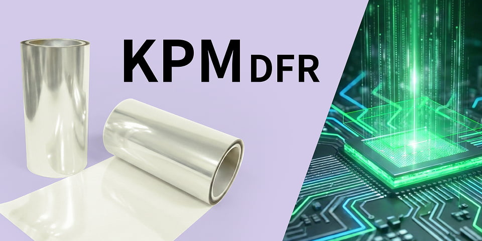
The KPM DFR Series is a dry film resist that enables both structure formation and substrate bonding with a single material.
Permanent dry film resists (DFR) allow uniform film thickness to be formed easily, enabling high-precision processing of fine patterns. They are also easy to handle and do not require waste-liquid disposal, which helps reduce environmental impact and lower operating costs.
Benefit 01
Benefit 02
Benefit 03
We design and manufacture our own epoxy resins optimized for use in photoresists, and these resins are incorporated into our dry film resists. The epoxy resins feature high purity and excellent electrical insulation properties. Their low-chlorine, low-halogen design helps prevent metal corrosion and insulation degradation. These resins provide both environmental compatibility and high reliability, making them suitable for manufacturing electronic components such as printed circuit boards and semiconductor devices. They also deliver high resolution and reliability in fine-pattern formation.
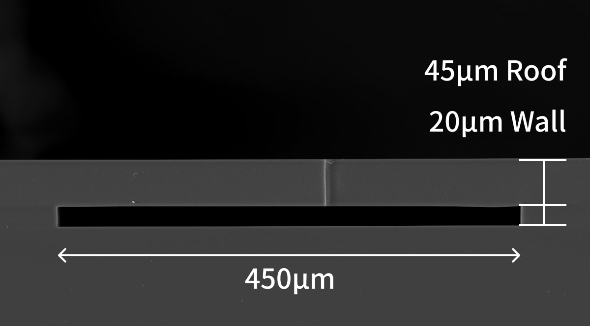
By laminating our SU-8 dry film resist (DFR) onto wafers using laminators manufactured by Teikoku Taping System (TTS), a Nippon Kayaku Group company, high-precision cavity structures can be formed. These cavity structures can serve as permanent structural layers in device fabrication. TTS laminators are equipped with patented Digital Bumper Technologies, which enable structure formation with both uniformity and reliability. The combination of SU-8 DFR and TTS laminators provides high-quality lamination suitable for next-generation electronic device manufacturing.
Patented Technology Enables Mass-Production Fabrication of Complex Structures

“Digital Bumper Technologies” uses elastic bumpers placed inside the laminator to optimally distribute pressure.
This design:
As a result, it helps prevent defects that can occur during lamination, such as uneven pressure, lifting or wrinkling of dry film resists, and bubble formation.

Liquid photoresists are photosensitive materials that enable the formation of fine patterns in the manufacturing of semiconductors and electronic components. Their liquid form allows uniform application by spin coating, enabling complex shapes and high‑precision patterning. They also provide easy control over film thickness, offering flexibility for a wide range of applications. As a result, liquid photoresists are essential materials in the production of high‑performance devices, including smartphones.